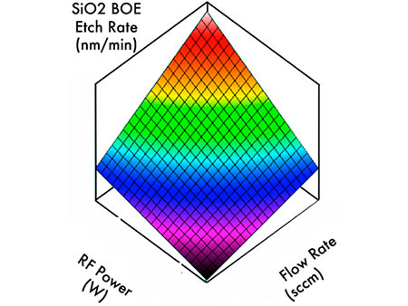
Processing solutions for the most widely-used photonic platforms: silicon (Si), silicon dioxide (SiO2), III-V semiconductors, and lithium niobate (LiNbO3)

Integrated optics market overview

A photonic integrated circuit, also called integrated optical circuit, is a device integrating several optical components that manipulate properties of light to perform complex photonic functions. Typical optical components include optical filters, lasers, lenses, and photodetectors, which are connected via optical waveguides

The primary application for integrated optical devices is optical fiber communication. Photonic devices can also be used in markets as diverse as spectroscopy, quantum computing, data storage, and imaging.

CORIAL solutions

Optical components are manufactured with technologies similar to those of electronic integrated circuits (photolithography, film deposition and etching). Integrated optics devices can be fabricated from a variety of substrate materials including lithium niobate (LiNbO3), silicon (Si), silicon dioxide (SiO2), nitride (Si3N4), and III-V materials (GaAs, InP).

CORIAL has extensive experience in developing processes for photonics devices, either including silicon, III-V and oxide based platforms.

AdvantagesCORIAL Advantages

R

Processes for the most widely-used photonic platforms

R

Equipment easily scalable from R&D to volume production

R

Cost-effective solutions

processEtch processes

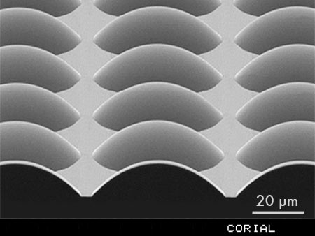
We have broad experience processing a wide range of materials with precise control of the etch profile, fast etch rates, and excellent etch uniformity.

Si etch by ICP-RIE for microlens structuring

  • Etch depth 30 µm
  • Etch rate 350 nm/min
  • Uniformity ±3%

SiO2 etch by ICP-RIE for microlens structuring

  • Etch depth 20 µm
  • Etch rate 400 nm/min
  • Uniformity ±3 %

InP etch for waveguide application

  • Etch rate > 300 nm/min
  • Selectivity vs. SiN > 20
  • Uniformity ≤ ± 3 %

processDeposition processes

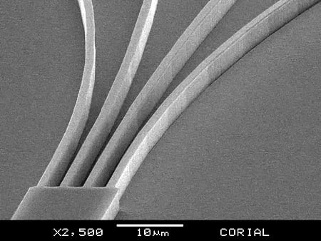
Planar waveguide layers can be formed using plasma-enhanced chemical vapor deposition (PECVD).

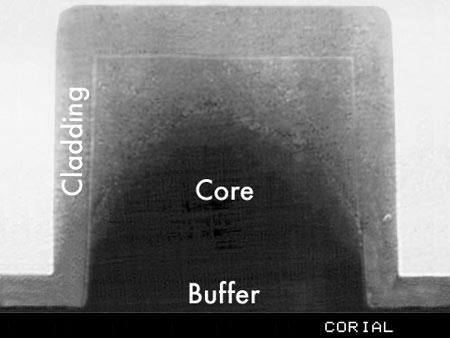
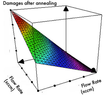
CORIAL offers deposition products and processes dedicated to the photonic market. These include PECVD deposition of intrinsic and doped SiO2 with excellent refractive index uniformity, minimum stress, and no Si-H bonds after annealing. We also offer PECVD deposition of the cladding layer with HMDSO for good step coverage.

Our equipment offers flexibility with many handling options and loading configurations. Additionally, all our PECVD systems with pressurized reactor deliver efficient in situ plasma cleaning without the need for manual cleaning of the reactor – and no pinholes.

Cladding layer deposition for Si waveguide

  • SiO2 PECVD rate 140 nm/min
  • Refractive index 1.46
  • Stress -280 ± 50 MPa

SiO2 layer deposition for passivation

  • Deposition rate 270 nm/min
  • Refractive index 1.46
  • Uniformity ± 3%

Low damage Si3N4 deposition on InP substrate

  • Deposition rate 20 nm/min
  • Uniformity ±3%
  • RF power 50 W

processProducts

Corial 210RL process

Corial-210RL-zoom
  • Flexible solution for reactive ion etching
  • Compatible with chlorinated chemistries
  • Silicon, silicon compounds, polymers, III-V & II-VI compounds and metals etch

Corial 210IL process

Corial-210IL-zoom
  • ICP-RIE etch system with load-lock
  • Fast etch rates for III-VI compounds
  • Cluster configuration for integration on the Corial PS200

Corial D250 process

Corial-D250-Zoom
  • PECVD system with in-situ plasma cleaning
  • High and Low-temperature PECVD
  • SiO2, Si3N4, SiOCH, SiOF, SiC and aSi-H films

Corial D250L process

Corial-D250L-Zoom
  • Same capabilities as Corial D250, plus vacuum load-lock for higher throughput