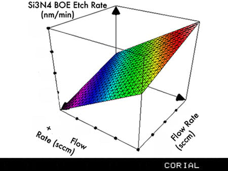
Exceptional process capability and flexibility, from damage-free processing of III-V to fast SiC etching and piezoelectric roughening

Wireless IC market overview

The Internet of Things, broadband data transfer, and more…It all becomes a reality thanks to modern wireless technologies.

The wireless market is dominated by compound semiconductor materials which are increasingly used to produce HEMTs, HBT, SAW and BAW devices.

CORIAL’s advanced dry etch technologies are capable of processing a wide range of materials used for to fabricate RF and MW active and passive devices.

CORIAL solutions

Our processing solutions offer rapid etching of SiC wafer and III-V semiconductors (GaAs, GaN) with precise shape control and low damage to the semiconductor structure. CORIAL’s products make possible the etching and surface structuring of piezoelectric materials such as lithium niobate and lithium tantalate which are widely used in SAW and BAW device fabrication.

CORIAL also delivers PECVD solutions dedicated to passivation of ICs and deposition of self-planarized dielectric coatings. Unprecedented uniformity of PECVD coatings makes CORIAL systems ideal for SAW and BAW passivation.

As device requirements continue to increase in complexity while shrinking in dimensions, Corial offers the added capability of atomic scale etching (ALE), for precise and damage-free etching of III-V semiconductor materials.

AdvantagesCORIAL Advantages

R

Broad application flexibility, from damage-free processing of III-V materials, to rapid etching of SiC wafer, and piezoelectric roughening

R

Clean processing with retractable liner that protect reactor, and collects etch by-products

R

One chamber for all wafer sizes

processEtch processes

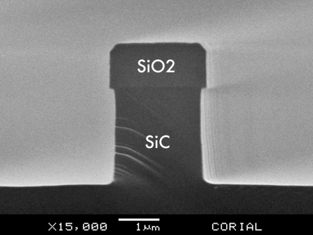
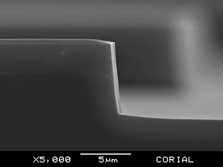
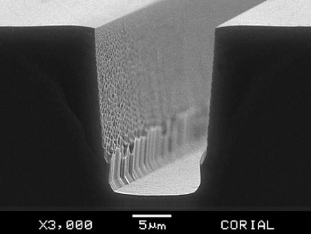
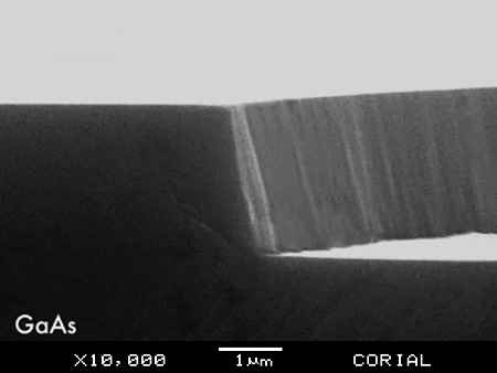
Wireless communication device manufacturing requires a range of etch processes, including via etch, low damage gate etch, mesa etch, and substrate etching.

ICP-RIE DRIE of SiC

  • Smooth sidewalls
  • Etch rate 0.7 µm/min
  • Selectivity vs mask > 2.5:1

InP mesa etch

  • Vertical profile
  • Etch rate 1.2 µm/min
  • Selectivity vs. mask > 50:1

GaAs via-hole etch

  • Etch depth 100 µm
  • Etch rate 8 µm/min
  • Etch profile 75°

GaAs mesa etch

  • Etch depth 2 µm
  • Etch rate 500 nm/min
  • Uniformity ±3%

process
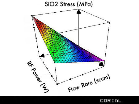
Deposition processes

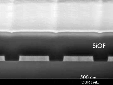
Wireless IC semiconductor applications require deposition of conformal interlayer dielectrics, passivation layers, and encapsulation films of various thicknesses, and on structures with different aspect ratios.

SiOF passivation layer

  • Deposition rate 65 nm/min
  • Refractive index 1.41
  • Stress -30 ± 50 MPa

SiO2 layer with tunable stress for passivation

  • Deposition rate 350 nm/min
  • BOE etch rate <240 nm/min
  • Stress 10 ± 50

High-quality Si3N4 film deposition

  • Deposition rate 110 nm/min
  • Refractive index 2.045
  • Stress -100 ± 50 MPa

processProducts

Corial 210IL process

Corial-210IL-zoom
  • ICP-RIE etch system with load-lock
  • Fast etch rates for III-VI compounds
  • Cluster configuration for integration on the Corial PS200

Corial D250 process

Corial-D250-Zoom
  • PECVD system with in-situ plasma cleaning
  • High and low-temperature PECVD
  • SiO2, Si3N4, SiOCH, SiOF, and SiC films

Corial D250L process

Corial-D250L-Zoom
  • Same capabilities as Corial D250, plus vacuum load-lock for higher throughput

Corial 360IL process

Corial-360IL-zoom
  • ICP-RIE etch system for 24/7 production environment
  • Load-lock for batch sizes up to 7 x 100mm wafers
  • Fast etch rates for sapphire, oxides and polymers

Corial D350 process

Corial-D350-Zoom
  • PECVD deposition system for 24/7 production environment
  • Manual loading for up to 300 mm wafers
  • High quality SiO2, Si3N4, SiOCH, SiOF, SiC and aSi-H films deposition

Corial D350L process

Corial-D350L-Zoom
  • Same capabilities as Corial D350, plus vacuum load-lock for higher throughput

Corial D500 process

Corial-D500-Zoom
  • Very large area PECVD deposition system
  • High throughput: 104x2’’ ; 25x4’’ ; 9 x 6’’ or plates up to 500 mm x 500 mm