The Corial D500 offers very high capacity process solutions for fast and uniform film deposition for batch sizes up to 104 x 2” wafers

Corial D500 PECVD system in brief

The Corial D500 PECVD system is designed to produce high quality, uniform films for power semiconductor devices, optoelectronics, and MEMS device manufacturing.

The PECVD deposition chamber is based on Corial’s unique reactor design. It houses an isothermal, pressurized plasma reactor located inside a vacuum vessel to enable efficient in situ plasma cleaning.

The combination of an optimized RF-powered showerhead with a dual-pumped system enables the deposition of dielectric films at high rates, while maintaining excellent film thickness uniformity.

The Corial D500 PECVD system offers high capacity batch deposition processing (104 X 2”, 25 X 4”, 9 X 6”, or 4 X 8”) for a wide range of materials at high temperatures (up to 325°C), including SiO2, Si3N4, SiOCH, SiOF, SiC and aSi-H films.

The PECVD tool can also be equipped with a chiller-based temperature management system. This option provides the capability to control substrate temperature from 50°C up to 150°C, with highly uniform temperature of substrate (±1 °C).


Key BenefitsKey benefits

R

EXCELLENT UNIFORMITY

Precise and uniform temperature control of the substrate and reactor walls delivers excellent deposition repeatability and uniformity

The pressurized, symmetrically-pumped reactor ensures high-quality films free of pinholes

R

HIGH DEPOSITION RATES

With its isothermal, pressurized reactor, the Corial D500 rapidly deposits uniform films on wafers up to 300 mm in diameter

Typical deposition rates: 320 nm/min for SiO2, 250 nm/min for Si3N4, 150 nm/min for SiOCH

R

LOW TEMPERATURE DEPOSITION

Default PECVD chamber supports film deposition from 120°C up to 325°C

Optional low-temperature chamber enables high-quality, low-damage film deposition at substrate temperatures as low as 20°C

R

INCREASED UPTIME

The Corial D500’s high temperature reactor walls and dual-pumped system enable efficient plasma cleaning at operating temperature, with no corrosion of mechanical parts

No manual cleaning of reactor and vacuum vessel required for many years of operation

Related processesRelated processes

Typical materials deposited with the Corial D500 PECVD system include silicon-based compounds such as SiO2, Si3N4, SiOCH, SiOF, and aSi-H.

The Corial D500 is specifically designed for volume production of films for power semiconductor, optoelectronics, and MEMS markets.

Silicon Nitride (Si3N4) PECVD deposition process with low RF

Silicon Nitride (Si3N4) PECVD deposition process with low RF

Silicon Nitride (Si3N4) PECVD deposition process with low RF

MEMS

  • Deposition rate 20 nm/min
  • Refractive index 2.00
  • RF power 80 W

Fast Silicon Dioxide (SiO2) PECVD deposition process

Fast Silicon Dioxide (SiO2) PECVD deposition process

Fast Silicon Dioxide (SiO2) PECVD deposition process

Optoelectronics

  • Deposition rate 110 nm/min
  • Refractive index 1.68
  • BOE < 650 nm/min

Silicon Carbide (SiC) deposition process at low temperature

Low temperature SiC PECVD deposition with tensile stress

Low temperature SiC PECVD deposition with tensile stress

Optoelectronics

  • Deposition temperature 80°C
  • Refractive index 3.00
  • Tensile stress 125 ± 50 MPa

Silicon Carbide (SiC) deposition process at low temperature

Stress less and low temperature SiC PECVD deposition

Stress less and low temperature SiC PECVD deposition

Power devices

  • Deposition temperature 80°C
  • Refractive index 2.91
  • Stress 10 ± 50 MPa

UpgradesIcon

The Corial D500 PECVD deposition system can be thoroughly customized with a wide range of features.

Additional gas inputs

Additional gas inputs

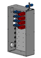
Additional gas inputs (up to 8) for more complex process gas combinations

Assisted loading

Assisted Loading

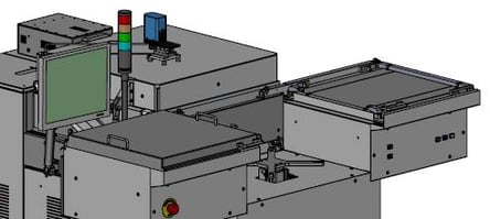
Mechanically-assisted loading system with heating and cooling stations for safe operation, to avoid handling damage to the wafers, and to ensure the highest throughput

Laser interferometry

End point detection by laser interferometry to enhance etch control through automated measurement of etch rate and etch depth

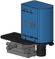
End point detection by laser interferometry to enhance process control through automated measurement of etch/deposition rate, etch depth and deposition thickness